
How Are USB Flash Drive and Memory Card Chips Manufactured?
Introduction
USB flash drives and memory cards have become essential storage devices in our digital lives, but few people understand how their core components – the flash memory chips – are actually produced. This article will explore the sophisticated manufacturing process behind these tiny yet powerful storage chips.
The Basic Structure of Flash Memory Chips
Flash memory chips consist of:
-
Silicon wafer substrate
-
Floating gate transistors (memory cells)
-
Multiple metal interconnection layers
-
Protective packaging
Step-by-Step Manufacturing Process
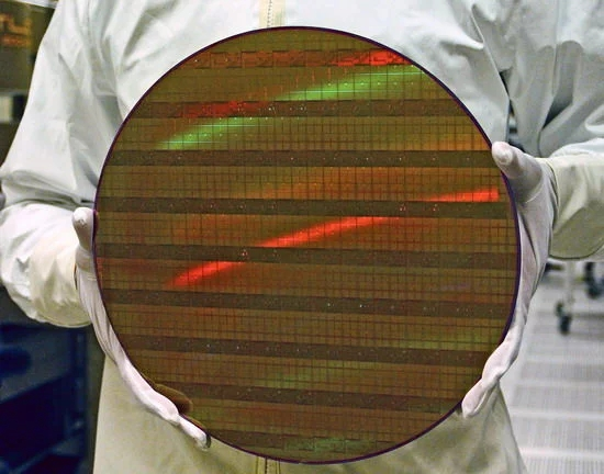
1. Silicon Wafer Production
The process begins with extremely pure silicon:
-
Silicon is refined from sand and purified to 99.9999% purity
-
Grown into single-crystal ingots using the Czochralski process
-
Sliced into thin wafers (typically 300mm diameter)
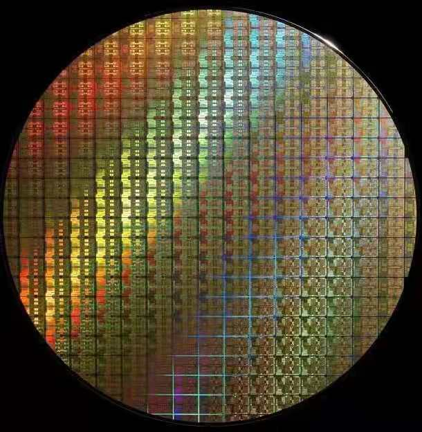
2. Photolithography
The wafer undergoes multiple photolithography steps:
-
Coated with light-sensitive photoresist
-
Exposed to UV light through a mask with circuit patterns
-
Developed to remove exposed/unexposed areas (depending on resist type)
-
Modern chips use EUV (extreme ultraviolet) lithography for smallest features
3. Etching and Deposition
-
Plasma etching removes unprotected material
-
Chemical vapor deposition (CVD) adds new layers
-
Physical vapor deposition (PVD) creates metal interconnects
-
This builds up the 3D NAND structure (for modern high-density chips)
4. Creating Memory Cells
Each cell contains:
-
Floating gate transistor structure
-
Charge trap technology (in newer designs)
-
Control gate, floating gate, tunnel oxide layers
-
Cells are organized in a grid pattern across the wafer
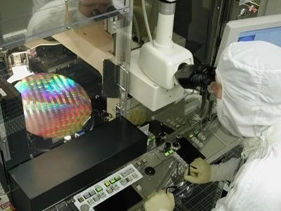
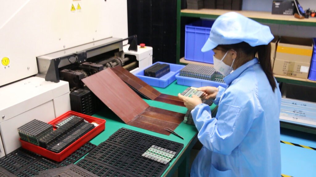
5. Testing and Quality Control
-
Electrical testing verifies each die’s functionality
-
Defective dies are marked and discarded
-
Only fully functional dies proceed to packaging
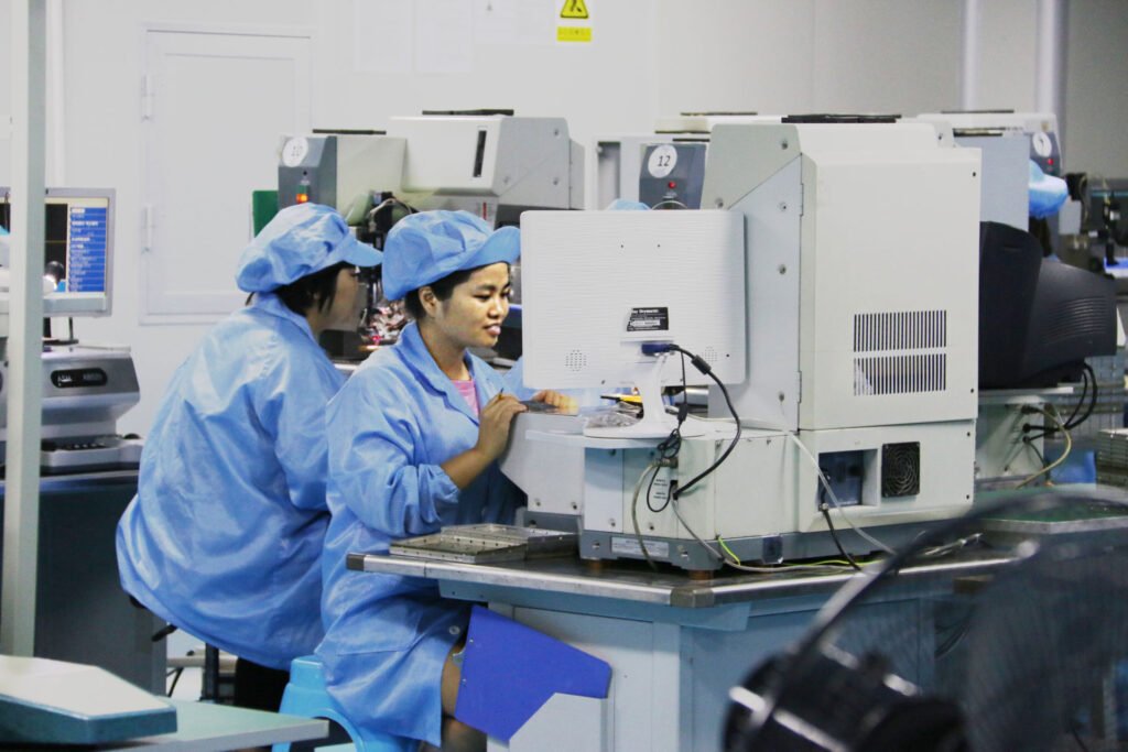
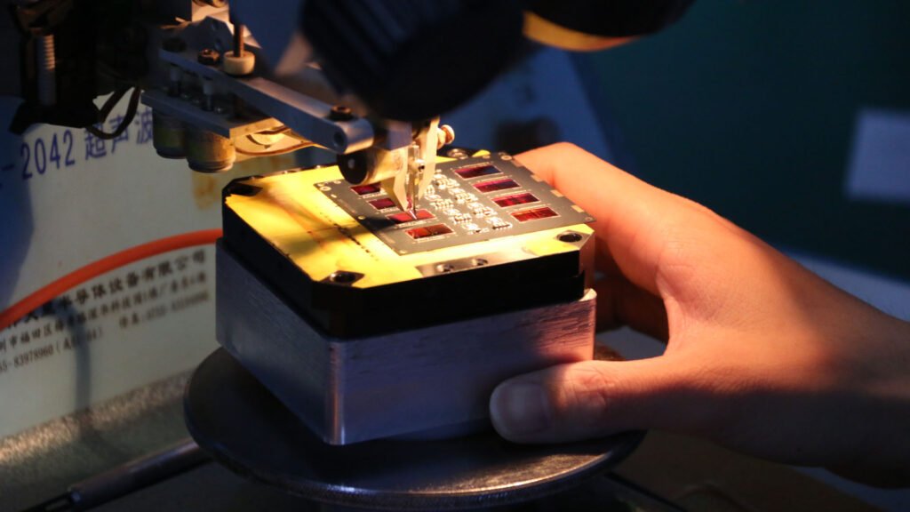
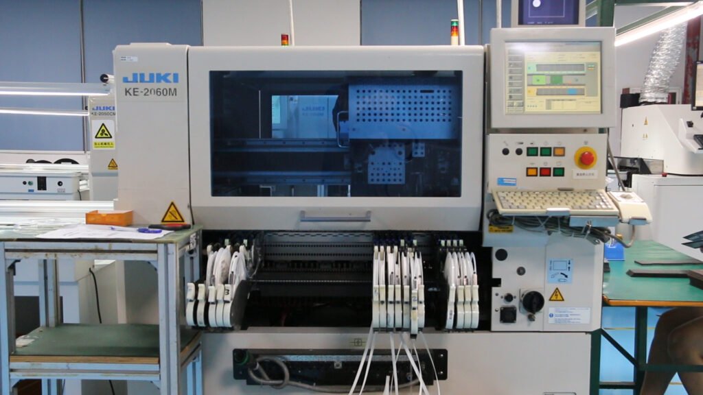
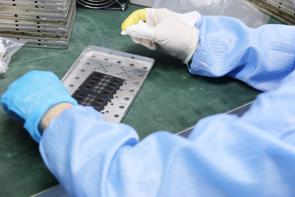
6. Packaging
-
Good dies are cut from the wafer (dicing)
-
Bonded to lead frames or substrates
-
Encapsulated in protective plastic
-
For USB/memory cards: additional controller chip is added
Special Considerations for USB/Memory Card Chips
High-Density Requirements
-
Uses 3D NAND technology with multiple stacked layers
-
Current technology reaches 200+ active layers
-
Enables terabytes of storage in tiny form factors
Endurance Optimization
-
Wear leveling algorithms in controller chips
-
Advanced error correction (ECC)
-
SLC/MLC/TLC/QLC tradeoffs between cost and durability
Future Trends
-
Transition to QLC (4 bits per cell) and PLC (5 bits)
-
Continued layer stacking (300+ layers)
-
New materials like ferroelectric RAM (FeRAM) in development
Conclusion
The production of flash memory chips is one of the most complex manufacturing processes in modern technology, requiring billions of dollars in fabrication facilities and nanometer-scale precision. This sophisticated process enables the affordable, high-capacity storage we rely on daily in our USB drives and memory cards.
Contacts
Abby ma
Whatsapp: +86 13049044451
Head Office
Shenzhen City,Guangdong Province,China
Support
supermemory.tech@gmail.com
Very useful knowledge!